Sony develops first stacked CMOS image sensor tech with 2-layer transistor pixel
New sensor technology is claimed to widen dynamic range and reduce image noise
The best camera deals, reviews, product advice, and unmissable photography news, direct to your inbox!
You are now subscribed
Your newsletter sign-up was successful
Sony has announced that it has "succeeded in developing the world’s first stacked CMOS image sensor technology with 2-Layer Transistor Pixel".
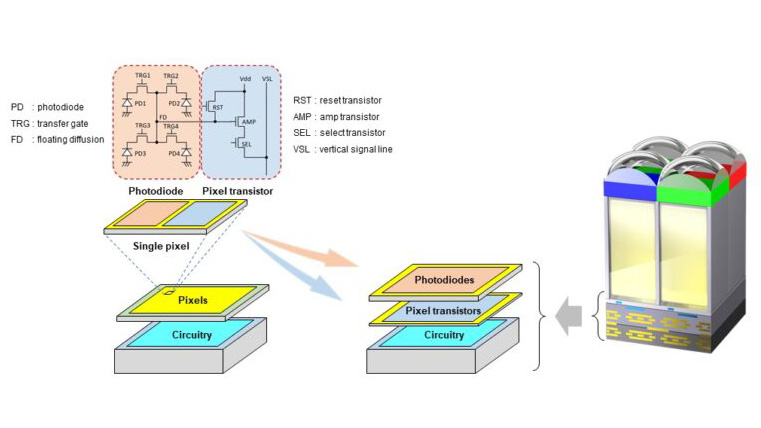
"Erm, what?" I hear you cry. Well, according to Sony, whereas conventional CMOS image sensors’ photodiodes and pixel transistors occupy the same substrate, this new technology separates photodiodes and pixel transistors onto different substrate layers. This allegedly has the potential to roughly double the saturation signal level compared to conventional CMOS sensors, resulting in enhanced dynamic range and reduced noise.
If this is sounding rather like deJa vu, then you're not alone. I recall vaguely similar claims being touted when the back-illuminated sensor was first released, and again when Sony introduced the first iteration of its stacked CMOS sensor at the launch of the RX100 IV and RX10 II cameras back in 2015. Since then we've seen a number of other 'world-first' implementations of stacked sensors in full-frame cameras and camera phones, each with incremental upgrades.
Article continues belowA 'conventional' stacked CMOS sensor is comprised of back-illuminated pixels stacked on top of a logic chip where signal processing circuits are formed. Within the pixel chip, photodiodes for converting light to electrical signals, and pixel transistors for controlling the signals are situated alongside each other on the same layer. Increasing saturation signal level within form-factor constraints plays an important role in realizing high image quality with wide dynamic range.
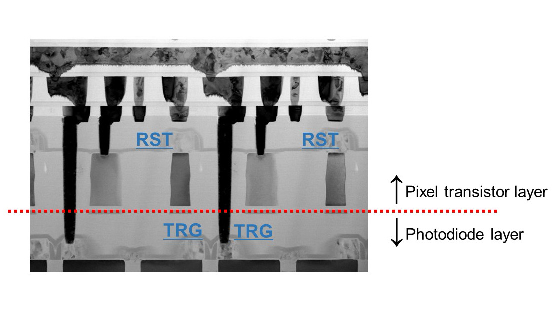
Sony has now modified this original stacked sensor structure by packaging the photodiodes and pixel transistors on separate substrates stacked one atop the other. In conventional stacked CMOS image sensors, by contrast, the photodiodes and pixel transistors sit alongside each other on the same substrate.
This new stacking technology allows the photodiode and pixel transistor layers to each be optimized, which Sony claims can approximately double saturation signal level relative to conventional image sensors and, in turn, can widen dynamic range.
Additionally, because pixel transistors other than transfer gates (TRG) occupy a photodiode-free layer, they can be increased in size. This in turn could reduce image noise in low light and night-time images.
The best camera deals, reviews, product advice, and unmissable photography news, direct to your inbox!
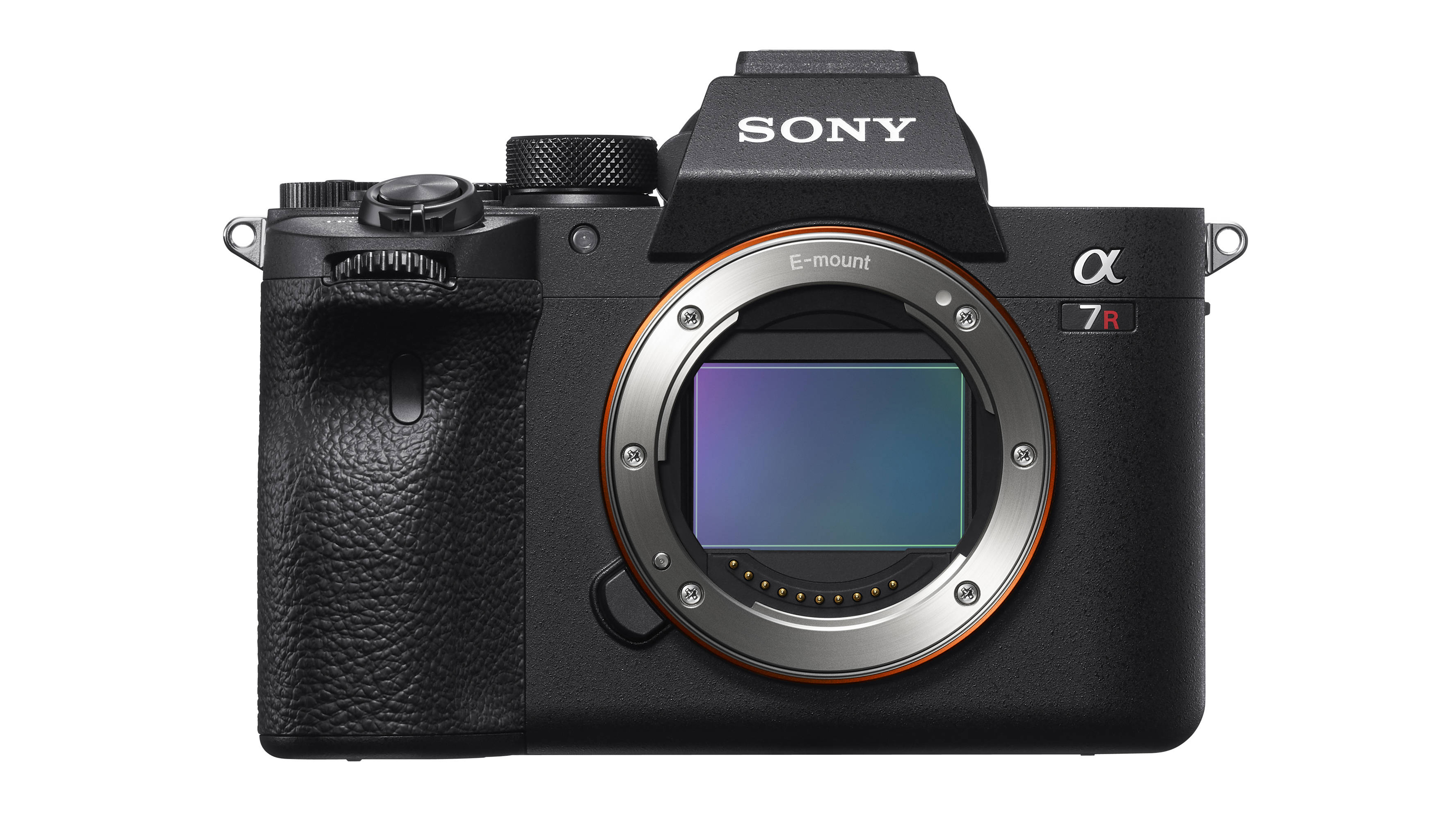
It's worth noting that Sony has only announced that it has developed this sensor "technology", which supposedly means an actual functioning sensor employing this technology may still be some way off. We'll have to sit tight to see if the 5th generation of A7/A7R is first to practically demonstrate 2-Layer Transistor Pixel technology.
Read more:
• These are the best Sony cameras to buy right now
• Best Sony lenses for full-frame and APS-C Sony cameras
• Discover the best lenses for Sony A6000 cameras
• Sony A7R IV vs A7R III vs A7R II : what are the differences?
Ben is the Imaging Labs manager, responsible for all the testing on Digital Camera World and across the entire photography portfolio at Future. Whether he's in the lab testing the sharpness of new lenses, the resolution of the latest image sensors, the zoom range of monster bridge cameras or even the latest camera phones, Ben is our go-to guy for technical insight. He's also the team's man-at-arms when it comes to camera bags, filters, memory cards, and all manner of camera accessories – his lab is a bit like the Batcave of photography! With years of experience trialling and testing kit, he's a human encyclopedia of benchmarks when it comes to recommending the best buys.
